Have you ever wondered how high-tech devices achieve such precise performance? The secret often lies in the tiny components that make them work.
Wafers play a crucial role in semiconductor manufacturing, affecting speed, efficiency, and reliability. Selecting the right wafer solution can transform a project's outcome.
Custom wafers offer flexibility to meet specific requirements and overcome production challenges.
They ensure consistent quality across every batch. By reading this blog, you'll learn how tailored wafer solutions can elevate precision manufacturing like never before.
Electronic circuits are built on wafers, which are very thin slices of semiconductor material. The most common material used to make them is silicon, but other materials may be used in some situations.
The wafer that the device is made from has a direct effect on how well it works overall. Wafers come in different diameters, thicknesses, and surface finishes so that they can meet a lot of different needs. In order to avoid mistakes, the process of making wafers needs to be carefully supervised.
To make sure that each wafer meets the standards of the industry, it goes through strict inspections. The basic properties of wafers affect how fast the device works, how much power it uses, and how long it lasts as well. Manufacturers can choose the right solution if they have a good understanding of these basic ideas.
This is not possible with standard wafers; custom wafer solutions are the only way to go. Changes can be made to them so that they work with unique device designs or production methods. Because these wafers are made to exact specifications, they help cut down on waste.
On top of that, they raise the overall yield and make the production process more efficient. Custom solutions can be used to deal with the problems that come up in high-performance applications. They often have coatings, dopants, and patterns that are made just for them.
The reliability of your device will be better if you choose a custom wafer. To put it all together, they give companies control over the quality and performance of the things they make.
The process of precision manufacturing relies heavily on the selection of the appropriate material. Silicon is the material that is most frequently used, but other materials such as sapphire or gallium arsenide are also utilized on occasion.
Both the electrical properties and the overall function of the device are impacted by the purity of the material. The presence of impurities can result in defects and decrease reliability. Processes of advanced purification are applied to wafers of high quality.
The choice of material also has an effect on the mechanical strength and heat resistance. When designing a wafer solution, engineers take these considerations into account. The selection of the appropriate materials guarantees both long-term performance and consistency.
Designing a wafer involves multiple factors, including thickness, diameter, and surface smoothness. The layout affects how circuits are fabricated on the wafer.
Manufacturers may require patterned silicon wafers to achieve specific functionalities. Surface treatments can enhance adhesion and electrical performance. Tolerance levels are critical for precision applications.
Custom designs can include etched patterns or layers for complex devices. Engineers must balance design requirements with cost and production feasibility. Thoughtful design leads to better device performance and reliability.
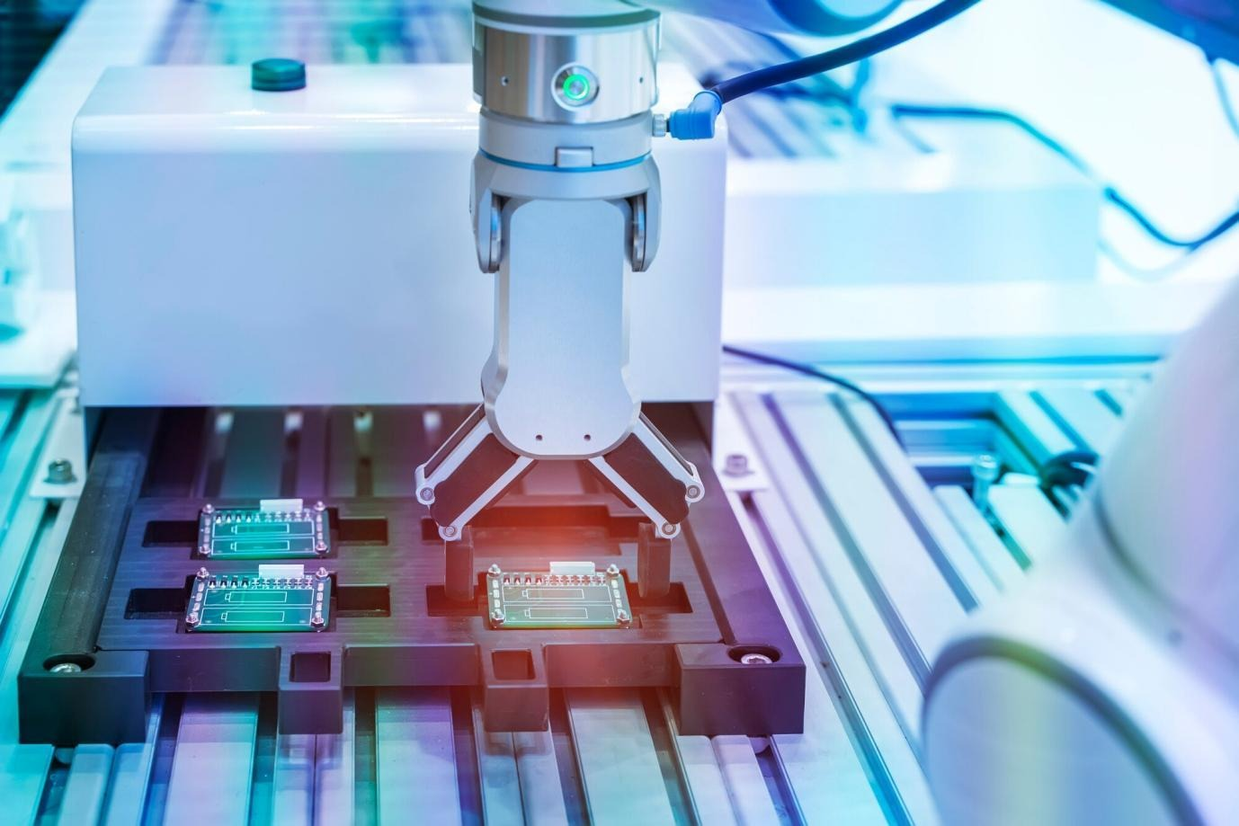
It is necessary to slice, polish, and clean wafers as part of the manufacturing process. When it comes to avoiding defects, each step needs to be carried out with precision. Continuous thickness and flatness monitoring is a common purpose for automated systems.
In order to enhance their properties, wafers may undergo either chemical or thermal applications. Waste is reduced and yield is increased when processes are optimized. Every batch is guaranteed to be consistent thanks to high-quality equipment.
For specific applications, manufacturers are able to tailor their processes. When production is optimized, the end product is wafers that are made to exact specifications.
With quality assurance, wafers work as they should in devices. We check for flaws on the surface, the thickness, and the electrical properties.
Consistent testing cuts down on application failures further down the line. Advanced imaging can find even small flaws. Manufacturers test based on standards set by the industry.
The results of quality checks make the next batches better. Regular inspections make sure that performance and dependability. Strong quality control is needed for precision manufacturing.
Custom wafers are used in many fields. Precise wafers are used in cars, medical devices, and consumer electronics. They are used in solar cells and other forms of renewable energy.
When used in aerospace technology, wafers are often very good at what they do. Specialized wafers can handle rough conditions. They make it possible to make parts smaller without affecting how they work.
Customized wafers are useful for all kinds of uses. The right wafer solution makes sure that the device works well and is reliable.
By making your own wafer solutions, you can cut costs. Higher yields mean fewer product defects and waste. Customized wafers make it faster to make devices. They cut down on steps in the process.
With efficient wafers, production goes up, and costs for labor go down. When something is reliable, it saves money on repairs and replacements.
Custom wafers give manufacturers the confidence they need to plan their production. They try to find a good balance between performance, cost, and efficiency.
Wafer technology is always changing. New materials have made devices faster, smaller, and stronger. Performance density goes up when 3D wafer stacking is used.
Sustainable ways to make things are being looked into. Sensors are being added to wafers more and more often. Customization lets businesses use these new ideas.
Stay ahead of the game by following trends. With new technologies, it will be possible to make things with more accuracy.
With custom wafer solutions, manufacturers have better control over quality, performance, and waste. They make it possible to carefully choose materials, design, and make the best use of production assets.
When things get really bad, these wafers make electronics and aerospace more reliable. Bundle consistency is guaranteed by testing and quality assurance.
Through higher yields and less waste, custom wafers save money. Manufacturers can get ready for new technology because they are flexible. Precise manufacturing is improved by customized wafers.
Did you like this guide? Great! Please browse our website for more!


Want to add a comment?